
Never Ignore the Importance of SMT Stencil

Introduction to SMT Stencils
A surface mount technology (SMT) stencil may also be called a PCB stentcil, solder paste stencil, or laser stencil. An SMT Stencil’s main purpose is to simply transfer the solder paste to a bare circuit board. A stainless steel foil is laser cut to create an opening for each surface mount device on the board. Once the printed circuit board (PCB) stencil is properly aligned with the top of the board, the solder paste is applied over the openings (in a single pass, with a metal squeegee). When the stainless steel foil detaches from the board, solder paste remains, ready for the manufacture of the surface-mount device (SMD). In contrast to manual soldering procedures, this process ensures consistency and saves time.

The deposited solder paste released to the board is manipulated by opening the size of the aperture, and the thickness of the SMT stencil is made out of stainless steel. Excessive paste will cause problems for connectivity and bridging, whereas less paste will compromise the strength of the soldering and joints.
The thickness of an SMT stencil varies with the device for which it is being used. 0.020” pitch small outline integrated circuits (SOICs) can work better with a stencil giving a thin solder paste, whereas thick solder paste works best with 0.050” pitch SOICs. The thickness of the paste stencil for solder ranges from 0.001” to 0.003”. The normal thickness for most of the PCB boards is generally between 0.004” and 0.007”.
Selective Sizes with PCB Stencils Are Now Offered with Nano Coating
For nano coating, the contacting sides of the tiny components are applied with a water-resistant nano coating that opposes solder and flux as well. This phenomenon results in the better release of paste for the tiniest components. The application is made in the factory so the component is ready to use at the time of purchase. The nano coating is recommended for fine pitches of QFN and IC, micro ball grid arrays (BGAs), and the electronic components of 0201 type.
The 6 most common varieties of PCB stencils, by size and type, are outlined below.

1. PCB Prototype Stencil
 Size: 10” x 12” max
Type: Squeegee
Add on: Board holder
2. Prototype Oversized Stencil (SMT)
Size: Over 10” x 12”
Type: Squeegee
Add on: Board holder
3. Kit-Leaded Prototype Stencil (SMT)
Size: 10” x 12” max
Type: Solder leaded paste
Add on: alcohol wipes x2, gloves x1 pair, temperature marker
4. Kit-Leaded Prototype Stencil Oversized (SMT)
Size: Over 10” x 12”
Type: Solder leaded paste
Add ons: alcohol wipes x2, gloves x1 pair, temperature marker
5. Prototype Kit-Lead Free Stencil (SMT)
Size: 10” x 12” max
Type: Solder lead-free paste
Add ons: alcohol wipes x2, gloves x1 pair, temperature marker, grab and place tool
6. Prototype Kit-Lead Free Stencil Oversized (SMT)
Size: Over 10” x 12”
Type: Solder lead-free paste
Add ons: alcohol wipes x2, gloves x1 pair, temperature marker, grab and place tool
Where Can PCB Stencils Be Made?

Framed stencils manufactured by stencils unlimited are easy to obtain. Upload your Cream Top from the desired PCB layout software after exporting it. After automatic calculation for the best suitable thickness of your stencil, send the stencil file to sale@aicom-electronics.hk; you will get a quote immediately .
If your PCB fabrication house can make stencils, they can also make stencils for you. A Gerber file is important for panel making. Don’t forget to ask them to make the GBC file if you want to make stencil yourself!
IPC 7525 has a detailed document about calculations of stencil thicknesses. The approximate value shall be 2.64 + 0.0831 * pitch-of-component.
PCBs revolutionized the electronics industry when they replaced the earlier method of circuit design on a chassis. Before PCBs, electronic circuit design involved bulky and loose components, such as connector lugs and screw terminals, which resulted in end products with large footprints and higher costs. By replacing manual point-to-point wiring, PCBs not only automated the process of circuit design but also greatly reduced the size of electronic end products.
Since the advent of PCBs in the beginning of the 20th century, it has gone through an evolutionary process of design improvements—such as transitioning from single-layer designs to 20+ layer boards. Overall, the PCB design process can be broken down into the following key steps:
- Electrical design
- Physical design
- Manufacturing
The manufacturing process is followed by the placement of components on the PCB called ‘board assembly’. Traditionally, the assembly process consists of following steps:
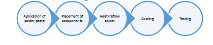
The Assembly Process with SMT Stencil
Conventionally, the board assembly process was performed manually placing and soldering the electronic components by hand. However, with the increasing complexity of circuit boards and extremely small sizes of surface mount packages, board assembly is moving towards application of solder paste using PCB stencils and machine-based component placement.
During the PCB assembly process, solder paste only needs to go where a component must be in electrically conductive contact with a metal landing pad on the board itself. The hand soldering method only makes sense where the design is simple, and the number of components is minimal. Naturally, hand soldering techniques are also prone to human error, which results in inconsistent results.
On the other hand, PCB stencils resolve these issues and are an effective and efficient method of applying solder paste. A stencil, as the name suggests, is a tool to make repetitive impressions. A PCB stencil acts as a guided template for the application of solder paste only on the desired areas of the board. The stencil is placed on the circuit board and aligned in the correct position. A runner is moved across the stencil screen which squeezes the appropriate amount of solder paste through the holes onto the circuit board.
Every stencil is customized according to the design of the PCB so that the solder paste gets applied only on the solder pads. For surface mount technology, the stencils are called SMT stencils. An SMT stencil consists of an outer aluminum frame, polyester mesh, and stencil foil. Stencil foil is tensioned and fixed to the aluminum frame by a polyester mesh.

How do you make a PCB Stencil ?
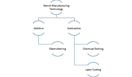
Typically, stencils are made of stainless steel or nickel and can be categorized based on the manufacturing process (process by which aperture is formed on the stencil foil), which follows.
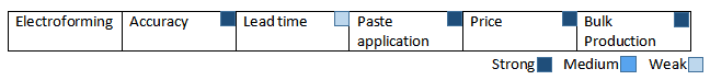
Electroforming: This is an additive process by which stencil foil is created by electroforming nickel. This process is also known as E-FAB. Although this process results in a higher initial cost,price is independent from the number of apertures. Finally, higher processing time is considered a drawback of this manufacturing process.
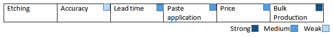
Chemical Etching:
This is a subtractive process by which apertures are achieved through chemical etching. This is relatively a low-cost process; however, it results in inferior results due to rough aperture sidewalls.
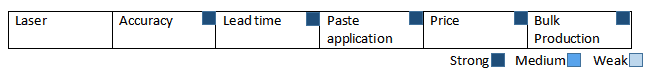
What is Laser stencil :
This is also a subtractive process by which removal of the stencil foil material is achieved by laser cutting. Naturally, laser cutting results in finer results and helps in achieving greater accuracy. Laser cutting also produces more consistent results than the chemical etching process. Since the process is not dependent on the chemical conditions, there is essentially no requirement for protection from moisture.
Depending on the method chosen for the application of solder paste, stencils can be further divided into following types:
Framed Stencils
These laser-cut solder paste stencils are permanently mounted on the frame where the border mesh provides the necessary tension to the stencil foil. These are designed for bulk machinery production.
Frameless Stencils
These stencils are not required to be permanently mounted on the outer frame. These low-cost stencils are recommended for prototype PCB assembly or short runs.
Prototype Stencils
Prototype stencils are designed for manual printing application. It removes the element of human error from the manual printing process.
Other Important Information
How to Generate a Stencil file from a PCB File
Generate a Gerber file from the PCB, and then send the Gerber file to the stencil manufacturer to make the stencil.
Generating a PCB Gerber file:
➤ Open the PCB file:open all layers in setup, then click view to confirm and save.
➤ Create a subdirectory: click on the file, use the drop-down arrow to select create in the pop-up dialog box CAM,andtype in the folder name, then click OK.
➤ Output Gerber file: Click Addand a dialog box pops up, fill in the drawing document name in the file name, use the drop-down menu to select the drawing type in the document field, and select the corresponding defined layer name in the pop-up dialog box. Define the output layer and the content of each layer at the level, click OK, then click Run.
➤ Output D code file: open the file and select the Gerber connection diagram at the top or bottom of the dialog box. The default values of each item in the dialog box pop up, thenclick OK.
➤ Output list file: Put all Gerber file lists into a folder, compress them into a compressed package, and save.
PCB Stencil Design Tips

Whether to get perfect and reliable solder joints, printing your stencil design is the key first step. The opening size of the surrounding pad stencil is directly related to the thickness of the stencil. Generally, thicker stencils can be designed with an opening slightly smaller than the pad size, while the opening size of the thinner stencil can be designed1:1. It is recommended to use a laser to make a steel mesh with openings and electropolishing.
◆ Stencil design of surrounding pads
The thickness of the stencil determines the amount of solder paste printed on the PCB. Too much solder paste will cause bridging during reflow soldering. Therefore, it is recommended that the 0.5mm pitch QFN package use a 0.12mm thick steel mesh, and the 0.65mm pitch QFN package use a 0.15mm thick steel mesh. The size of the stencil opening can be appropriately smaller than that of the pad to reduce the occurrence of solder bridging.
◆ PCB Stencil design of heat dissipation pad
When the exposed pads on the bottom of the chip are soldered to the thermal pads on the PCB, the gas in the thermal vias and large-size pads will overflow outwards, resulting in certain air holes. Therefore, if the solder paste area is too large, it will produce various defects (such as sputtering and solder balls, etc.). However, it is almost impossible to eliminate these pores;it is possible only to minimize the pores. When designing the stencil in the thermal pad area,careful consideration is needed.
It is recommended to create multiple small openings in this area instead of one large opening. The typical value is 50% to 80% solder paste coverage. Practice has proved that the solder joint thickness of 50μm is very helpful to improve board-level reliability. In order to achieve this thickness, it is recommended that the solder paste thickness for the underfill thermal via design beat least 50%; for the through hole, the coverage rate is at least 75% the above.
How to clean an SMT Stencil
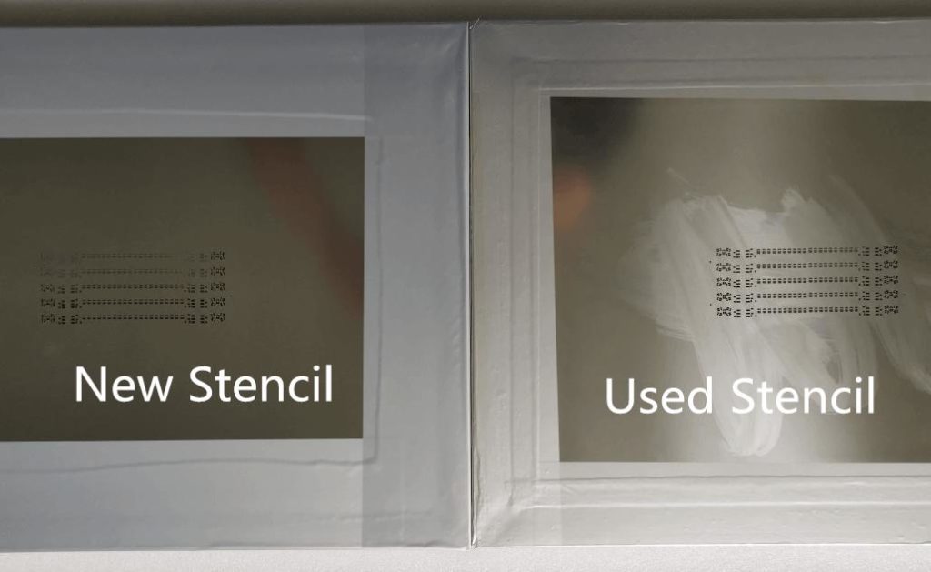
SMT stencils are generally cleaned with professional cleaning equipment. Presently, the mainstream of the market is the smart stencil cleaning machine, which is aimed at the electronic industry SMT stencil, copper stencil, wire stencil, microporous stencil, and wafer trays. For the cleaning of similar stencils, the equipment uses compressed air as energy, does not require electricity, and is not a fire hazard.
It adopts a human design and one-button operation, which helps complete cleaning and drying tasks; it utilizes high performance automatic operation of air pressure. As for cleaning equipment, the cleaning fluid is recycled, with low loss. click to know more about how to clean smt stenicl .
SMT Stencil Manufacturers List:
China and India have a strong base of SMT stencil manufacturers. Here is a list of few suppliers based in different regions around the globe:
| Region | Country | Company |
| APAC | China | Aicom Electronics PCB |
| APAC | Australia | MasterCut |
| APAC | China | Found Printed circuit Board Co. |
| APAC | China | MorePCB |
| APAC | China | PCB Sino |
| APAC | China | JLC PCB |
| APAC | China | PCB Way |
| APAC | China | ALL PCB |
| APAC | India | Satchitanand Group |
| APAC | India | Asahitec |
| APAC | India | Stencil Point |
| APAC | India | Kristeel-shinwa |
| Europe | Germany | LPKF |
| Europe | Germany | Becktronic |
| Europe | Germany | Koenon |
| Europe | Italy | ALBA PCB |
| North America | US | Tropical Stencils |
| North America | US | Stencils Unlimited |
| North America | US | EPEC Engineering |
| North America | US | OSH Stencils |
Top 10 PCB Stencil Factory in Europe
Are you looking for the best PCB stencil manufacturer in Europe? There are lots of them. With 44 countries in the continent, rest assured that you can find or more stencil PCB factories to handle your circuit board project in Europe.
The challenge, however, is how to find out the best stencil PCB manufacturers. With lots of them, you may be confused about the factory that offers the best service.
Also, you want to consider other important factors, such as the type of stencil PCB service the factory offers, the cost of their service, and the turnaround time.
You can be confident now knowing that you are reading a guide that will walk you through the entire process.
This article is about the 10 leading SMT stencil factories in Europe. It is also about some of the reasons why we selected the manufacturers on the list.
What is SMT Stencil?
Let us understand what an SMT stencil means before we proceed to show you some of the stencil PCB printers you can find in any of the European countries.
An SMT stencil is known by many other names. It can be called Laser Stencil, PCB Stencil, or Solder Paste Stencil. We are pointing this out so you don’t become confused when you come across how we interchanged the names in the course of reading this guide.
An SMT Stencil is the process of transferring the solder paste to a Printed Circuit Board (PCB). This is done because the process of designing circuit boards (PCBs) can be a bit complicated.
So, it is pertinent to ensure that the solder paste required for modeling the board the way it should be is done the right way. That is what the stencil PCB is used for.
Worthy of mention is that the stencil PCB process is mostly used when using the Surface Mount Technology (SMT) to design Printed Circuit Boards (PCBs).
Besides, the mounting or placement of the Surface Mount Device (SMD) needs to be accurate. For this to go on as expected, a stainless-steel foil would be laser cut. The aim of doing this is to create an opening on the circuit board. This way, it would be easier to mount or place the Surface Mount Device (SMD) on the Printed Circuit Board (PCB).
The 10 Best Stencil Factories in Europe
Here is the subject of this guide – the top European PCB manufacturers that specialize in stencil PCB.
We selected these factories or PCB manufacturing companies based on many criteria, including the years of experience, the quality of their stencil PCB service, and the overall customer satisfaction.
You can, therefore, be confident that you would get the best stencil PCB service and value for your money.
When you have a stencil printing project, these are some of the best factories to contact in Europe:
1. PHOTOCAD
Some top European PCB manufacturers offer a wide range of circuit board design services, including stencil PCB.
However, others focus on just stencil PCB. For this type of circuit board factories or manufacturers, their goal is to provide an all-around stencil PCB service.
One of such manufacturers is PHOTOCAD. It is a German step stencil SMT manufacturer that takes orders for different kinds of SMT stencil products.
It is imperative to mention here that PHOTOCAD has an eye for details. And as their slogan suggests, they ensure that “precision works” in all of the stencil PCB solutions they offer.
Services
The company also offers a variety of step stencil design services that are targeted at different kinds of customers.
For example, there is an option for manufacturing SMT stencils that are optimized for the smallest components.
Likewise, the factory offers a Basic Plan service that has to do with the production of stencil PCBs by using standard applications.
SMT Stencil Technology
The process of manufacturing the SMT stencil is also commendable. The manufacturer uses high-precision stencil technology as a way of ensuring that the stencil printing process step by step is achieved.
The company also delivers optimum results for circuit board assembly and solder paste printing. This is done by offering additional surface finishing solutions for the stencil circuit boards. The common solutions used here are electropolishing and nano-cutting.
By and large, you would love to hire PHOTOCAD to handle your step stencil SMT printing because of the excellent service the factory offers.
Some of the other reasons why you want to partner with them are:
- Providing a wide range of storage systems and solutions
- Optimal configuration for your stencil SMT
- The use of standard and more sophisticated SMT stencil technology
- Individualized SMT stencil solutions
- Affordable step stencil design
Website: https://www.photocad.de/en/
2. Becktronic
Germany has one of the largest concentrations of PCB stencil printer factories. So, if you are looking for where to get the service cheaper and ready in the shortest time possible; go to Germany.
We have yet another largest PCB manufacturers in Germany. The name of this manufacturer is Becktronic and it is your one-stop provider of full-scale SMT stencil services.
Becktronic offers an optimized or personalized stencil printing service. This way, you can get the best out of your SMD stencil.
This is not leaving out the fact that this PCB manufacturing Europe service provider is also committed to offering you the best service. This is why you can be sure of getting other options, such as choosing to optimize your stencil printing based on a wide range of grid dimensions and templates.
Individual SMD Stencils
Going for the individual SMD stencils option is one of the best ways to get the best out of your stencil printing.
Becktronic offers this stencil SMT service because it understands how important it is in terms of being a basis for precise solder paste printing.
The individual SMD stencils solutions offered by the company are not only competent and reliable as it pertains to your requirements for the printing. The other impressive factor is that the manufacturer (Becktronic) takes charge of most of the processes, starting from the optimal execution of the SMD stencil to the assurances of consistency in the quality control process.
In addition to all that, Becktronic also offers professional or personal advice. This is done to help you and the other customers to find and choose the right SMT stencil solutions.
Website: https://www.becktronic.de/
3. Quick-teck
Quick-teck is a PCB stencil factory located in Hertfordshire. The company prides itself to be the “Low-Cost UK Circuit Board Manufacturer.”
But that is not the main value that the company delivers. The main value is that asides from the PCB design services, the factory also accommodates stencil PCBs. This way, it offers a broad range of SMT stencil services that are targeted to cater to the needs of different kinds of customers.
The Laser Stencil is the most common stencil printing that it offers. For this, the stencils are made of stainless steel and would be cut for printing the solder pastes.
The customers are also allowed to select either the stencil sheet or the framed stencil. The one they selected would then be shipped together with the Printed Circuit Boards (PCBs).
Several specifications are applied to the laser stencil solutions offered by Quick-teck. Some of these specifications include:
- The use of laser technology
- Hardened special steel material is used for the design
- The SMT stencil would be subjected to a surface finishing before it would be shipped
- Four fiducials at each corner
- You can also get free shipping
Why Should You Choose Quick-teck for Your PCB Stencil Solutions?
Thousands of customers have patronized this stencil printing factory in Europe. A majority of those customers are satisfied with the services they got. We are sure you will feel the same way after letting Quick-teck handle your laser stencil.
Here are some of the reasons why you should consider working with them:
- The factory safeguards your intellectual property by providing a Non-Disclosure Agreement (NDA).
- The factory can take minimum orders, as low as 1 low-cost RoHS Compliant PCB prototype.
- They also offer on-time delivery. Ideally, they offer a standard lead-time of 9 working days maximum for low production orders and up to 5 weeks for large volumes.
Website: https://www.quick-teck.co.uk/
4. Multi-Circuit-Boards
The quality of the Multi-Circuit-Boards services in the circuit board market is not in doubt. As much as the factory is diversified, it still has considerable control and a mastery of the different kinds of PCB designs and production processes. The stencil SMT process is also inclusive.
As the name of the manufacturer signifies, it focuses on the provision of services across multiple Printed Circuit Board (PCB) markets. It doesn’t matter if you are looking for PCB design or circuit board prototypes. It does not also matter if you are looking for SMD stencils or toroidal transformers.
Whatever it is you are looking for, rest assured that Multi-Circuit-Boards has got you covered. Since we are looking for PCB stencil printer services, let us see how the factory can help us out.
SMD Stencils
This is one of the stencil SMT services that Multi-Circuit-Boards offers. The solder pastes and adhesive stencils (SMD Stencils) are one of the most important requirements for any Surface Mount Technology (SMT) to be successfully used to place Surface Mount Components (SMD) on a circuit board.
One of the unique attributes of the SMD Stencils from Multi-Circuit-Boards is that it is usually manufactured using laser technology. The use of this technology is the reason why the Stencil SMT solutions from Multi-Circuit-Boards have higher precision and maintain consistent quality.
Multi-Circuit-Boards also offers several other services that make it one of the top European PCB manufacturers. These services include but are not limited to:
- Deburring/double-sided brushing
- Unlimited pads
- Final treatment, such as nano protection and electropolish
- Up to 8 fiducial marks
- Edge protection
- Pad manipulation
Website: https://www.multi-circuit-boards.eu/
5. NewburyElectronics
NewburyElectronics is your one-stop PCB manufacturing company that offers a one-stop Electronics Contract Manufacturing (ECM). This means that you wouldn’t necessarily need to look for additional ECM services elsewhere because everything is offered in-house by NewburyElectronics.
The factory also offers unparalleled Surface Mount Technology (SMT) Assembly services. These SMT services are offered for a wide variety of industries. So, you can be confident that the factory would come up with impressive solutions for your SMT stencil needs.
What we find fascinating about the SMT stencil solutions offered by the manufacturer is the fact that it doesn’t stop at anything when it comes to delivering quality.
This is why NewburyElectronics would spend both time and money to purchase state-of-the-art machinery that would be used to facilitate the design and production of SMT stencils.
This is not forgetting the fact that the factory takes the quality control of the stencils seriously. This informs the reason for the rigorous implementation of process control to ensure that the stencils work as they should.
Solder Paste Stencils Production
The most important thing we would like you to take note of is that NewburyElectronics is a solder paste stencil manufacturer. As such, it is one of the best PCB stencil manufacturers you should consider consulting in Europe for your stencil SMT needs.
NewburyElectronics uses the laser cut solder paste service to provide Stencil SMT services to customers who either need the screenprinting of the solder paste onto the circuit boards or the assembling of the surface-mounted components required for the mounting procedures.
Website: https://www.newburyelectronics.co.uk/
6. Prima-Tech-Pro Ltd
Prima-Tech-Pro Ltd is one of the leading PCB stencil factories in Europe. The company was established in 1996 to introduce new concepts in the design and development of electronic components and Printed Circuit Boards (PCBs).
That notwithstanding, the company has been able to rise through the ranks to become one of the most patronized Printed Circuit Board (PCB) manufacturers in Bulgaria.
Today, Prima-Tech-Pro Ltd offers a wide range of circuit board design and development services, including but not limited to the design and supply of metal stencil PCB, PCB assembly, and the supply of electronic components.
It will also interest you to know that the factory or company places a premium on the design and development of stencils. This is why they keep innovating and investing in some of the best and latest Surface Mount Technology (SMT) equipment. The idea is to be a step ahead of the competition and to offer improved technical capabilities, as well as increasing the production capacities.
In terms of the PCB stencils, there are a couple of things we would like you to know about Prima-Tech-Pro Ltd. The first is that the factory has invested and is currently one of the latest models of the Pick & Place machines. The machine plays an important role in the speed and the accuracy of the circuit board production services offered by the company.
The second is that Prima-Tech-Pro Ltd doesn’t charge you an arm and a leg. Ideally, the competitiveness of the labor costs attracts more customers to the company. And to make it more enticing, the factory operates a transparent pricing policy, which makes it easier for the customers to find out if there are hidden costs or not.
Third and most important, Prima-Tech-Pro Ltd uses laser cutting technology as a way of facilitating the design and supply of metal stencils. This way, excellent productivity, and quality would be ensured in the production process of those stencils. This is not leaving out the fact that the PCB stencil printer services offered by Prima-Tech-Pro Ltd also encourage faster delivery without any compromise in the quality or the accuracy of the SMT stencils.
Website: http://www.primatechpro.com/
7. AssemTecEurope
AssemTecEurope is one of the other PCB manufacturing companies that offer SMT stencil designs and production in Europe.
It is interesting to note that the company specializes in the contract assembling of both Surface Mount Technology (SMT) and Through-Hole Technology (THT).
The idea is to ensure that the production of any kind of electronics or circuit board is done with the right kind of equipment. And AssemTecEurope has lots of them to ensure that the production is done with the latest technologies and equipment.
In terms of SMT stencils, this manufacturer does a lot to make them attractive to potential customers. For example, AssemTecEurope offers assistance in the preparation of projects for electronics assembly. Worthy of mention is that the manufacturer sees to the application of the reference points, which is required to fine-tune the software that would be used for SMT.
Electronic Components Assembly
In terms of the assembly of electronic components via SMT, AssemTecEurope does its best. Among many other things, the manufacturer glues the Surface Mount Device (SMD) elements, especially when they have to do with the double-sided assembly of larger elements.
Second, AssemTecEurope sees to the automation of the Surface Mount Devices (SMD). Both the single and the double-sided SMDs are automated in this case.
Third and most important, the stencil PCB process offered by AssemTecEurope is often subject to reflow soldering in a convection oven.
The manufacturer (AssemTecEurope) also does a great job of ensuring quality control throughout the process.
Website: https://assemteceurope.com/
8. EverMax
EverMax offers an extensive list of electronic device production services and a majority of these services are based on the automatic mounting of Surface Mount Devices (SMD) components.
Thus, they are one of the best PCB stencil factories in Europe that can automate the entire process of placing or mounting Surface Mount Devices (SMD) on the circuit boards.
Automatic Screen Printing
EverMax also offers automatic screen printing. In this case, we are looking at the use of a fully automatic screen-printing machine that would be used to automate the quality and the accuracy of the proofing for the solder paste to be mounted on the circuit board.
The automated screen-printing process also comes with an extra level of precision. Ideally, the screen-printing machine used by EverMax comes with the HawkEye (TM) function. This is a modern function used for enabling an optical inspection of the printed solder paste. This is done to ensure that the paste is of high quality, as well as to examine or have an overview of the surface of the circuit board that the paste would be mounted on.
Mounting Device
EverMax also has a specialized mounting device called AdVantis AC30. The machine was sourced from Universal Instruments and is used for mounting the stencils on the circuit board.
Website: https://www.evermax.cz/
9. Alba PCB
Alba PCB specializes in the production and servicing of different types of Printed Circuit Boards (PCBs).
This notwithstanding, the company does play an important role in the advancement of the PCB industry. This is evident in the effectiveness in the area of offering Surface Mount Technology (SMT) laminate services.
In this case, the manufacturer offers SMT stainless-steel furnishing for SMT sheets. The steel would be used alongside the laser cutting technology to facilitate the spread of the soldering paste.
Also, Alba PCB offers the customers the opportunity to decide on the type of sheet they want. The two major options are the production of the SMT sheets with aluminum frame (silkscreened frame) and the production of simple SMT sheets that would be used for self-tensioning frames, including ZELFLEX, and DEK VectorGuard.
Website: https://albapcb.com/
10. Euro Circuits
We saved the best for the last. Euro Circuits is one of the leading manufacturers of different kinds of Printed Circuit Boards (PCBs) in Europe.
They are also one of the best when it comes to stencil printing in Europe. Ideally, the company offers you two options to choose from, as far as laser-cut stainless-steel solder paste stencil is concerned.
The first option is to choose the custom solder paste stencils and the second is to choose the eC-Registration compatible solder paste stencils.
Both are laser cut from 100 to 130-micron stainless steel. You also have the opportunity to choose the stencils together with the Printed Circuit Boards (PCBs).
Website: https://www.eurocircuits.com/
Concluding Thoughts
Stencil PCBs are in high demand because of the precision they bring to the table. Likewise, more PCB consumers in Europe are looking for the best stencil factories to do the job for them. The list above discussed the 10 leading PCB stencil factories you can find in Europe.
But Europe is not the only continent where you can find the best SMT stencil factories. There are more of these factories in Asia and China to be precise. When you look in this direction, contact Aicom Electronics PCB (one of the best PCB stencil printers in China) to deliver the solutions you want.
3.Bad block and ECC
The occurrence of bit flipping is random, and the number of bit errors will increase as the number of erasing and writing increases. But as long as the number of bit errors is within the range that ECC can correct, data integrity is always guaranteed. At some points, the bit error of each page may be very close to the limit that ECC can correct. The NAND control system must strictly prevent the bit error from exceeding the correctable range. Otherwise, data may be lost, or the system may not work normally. Therefore, these blocks must be marked as bad blocks.
Bad blocks should never be used to store data again. Because the generation of bad blocks is inevitable, NAND manufacturers will choose to mark certain blocks as bad blocks when testing the die rather than abandon the entire die. Therefore, most NANDs are already marked as bad when they leave the factory. Block of blocks. If a NAND block is marked as a bad block, then the NAND’s capacity is permanently reduced.
2.The key points of And system die mass production and burning
Due to the NAND Flash chip characteristics, they must be processed appropriately when using it as a storage medium so that the system can operate normally. The system sets the storage layout of each partition data in the NAND chip and performs bit error correction and bad block management on the Nand at the storage drive layer. This information needs to be clarified by the system/drive engineer.
In the R&D stage or small batch production stage, the method of programming is often used. The principle is to download the boot to the memory through the serial port and run, and then the boot will burn the kernel image, file system image, and other data from the SD card or network to the NAND Flash chip.
In order to improve production efficiency or other considerations, a writer will be used to mass-produce NAND Flash dies. Since the writer manufacturer does not know how the storage driver layer handles various characteristics of NAND, it is unreliable. If the programming is performed after configuration, the following situations often occur:
1. The programming fails, often because of the verification failures.
2. The programming passes, but the system cannot run after some chips are mounted on the board, or some modules appear when running with errors and exceptions. Most of these are not the burner’s problem, but that several important key points are not handled correctly when the NAND system is burned on the bare chip. Another reason might be the processing is not consistent with the target system. These key points include:
- Bad boards solution
2) Partition
3) Error Correction Codes,ECC
Other factors affect the burning, such as spare area usage, unused fast formatting, dynamic metadata, etc. Still, we will only discuss the above few more common factors here.
- Bad boards solution
Bad boards are generally identified according to the bad block mark position of the chip, and the bad boards processing strategy defines how the algorithm should deal with bad blocks. The strategy algorithm is responsible for writing the content that should have been written in the bad block to other optional good blocks. The most commonly used bad block processing strategy is to skip bad blocks. Other typical bad block skips with BBT and reserved block areas.
The processing strategy of skipping the bad board is the most basic and most commonly used bad block replacement strategy. When a bad block is encountered during programming, the algorithm skips the bad block and writes the data to the next good block. It will cause the location of physical data and logical data to shift, which usually requires partitioning to solve this problem.
(2) Partition
The NAND system, which adopts the processing strategy of skipping bad blocks, often divides the storage into several different physical areas. This is what we call the partition, which is conceptually similar to the partition of a computer hard disk.
Using partitions gives you the ability to ensure that your data can be stored in a pre-specified physical block area, even if some bad blocks are found before that. This helps low-level software components such as bootloaders and certain file system drivers that must be easily located.
When the replacement strategy of skipping bad blocks is used, the bad blocks will cause the data to move to the next good block. If the partition is set, you can instruct the writer to determine the boundary of the data to ensure that the data file will not encroach on the adjacent partition.
Figure 2.2.1 is the partition situation of a typical embedded Linux system.
(3) Error Correction Codes,ECC
It is necessary to adopt appropriate ECC algorithms for NAND storage systems of different processes and capacities. It is even necessary to ensure the reliability of the system. ECC error correction codes are generally stored in the spare area and are calculated from the data of a whole page or divided into several sections. Before data programming, ECC (except hardware ECC) needs to be prepared. If it is pure data, it needs to use the ECC algorithm to generate.
In mass production of NAND bare chips, it is important to know the error correction capability (error correction bits) of the ECC algorithm. To ensure production efficiency, it is impractical for the programmer to use ECC to verify the data. Through simple Data comparison, it can know the number of bit flips of the data. If the range of the number of flips is within the error correction range of the ECC algorithm, it is considered that the check should pass.
3 Customized Programming
For the above key points, if the writer software does not support the corresponding program, you need to contact the original factory to customize the relevant algorithm, such as bad block processing program, ECC program, etc.
Sixth MCU programming solution
MCU type can burn IC. Many single-chip controllers (SINGLE MCU) on the market can be used to burn one or more data through the matching burner. Usually, the MCU that can be programmed only once is called OTPMCU (English: ONE TIME PROGRAMMABLE MCU). In contrast to MTP, MCU (English is MULTI TIME PROGRAMMABLE MCU) is an MCU that can be programmed multiple times.
OTP MCUs are usually burned in by the manufacturer at one time through the matching burner before the product is assembled. Once this type of IC is burned, the burned data cannot be changed again.
MTP MCU is different from OTP MCU. This type of IC can be programmed and erased multiple times through the matching programmer. Some of the built-in FLASH MCUs can even be programmed not less than 100,000 times.
Programming room environment
Chips are electrostatic-sensitive components, so anti-static measures must be taken
(1)The electrostatic grounding wire of the chip room should be connected to the ground, not directly connected to the grounding wire of the power supply. The ground resistance of the electrostatic grounding system should be less than 0.5 ohm.
(2)Employees in the chip room should wear static wristbands and anti-static clothes when programming chips, and anti-static table mats should be laid on the work surface.
(3)The staff in the chip room must use the static ring tester to measure whether the static ring is good and the wearing specifications before officially burning the chip every day. It can not officially put into production until everything is normal.
(4)The OTP room has an anti-static grade of A, and the absolute value of static should be less than 100V.
- Humidity greatly influencesstatic electricity, so a humidity tester should be added to the chip room for control. The best humidity range should be 50%-60%. If the humidity is low, you can use a humidifier or touch the ground. Sprinkle water to control the humidity within a proper range.
Best IC Chip Programmer and Tutorial
1. Renesas chip M37544, M37546, M38503 program burning:
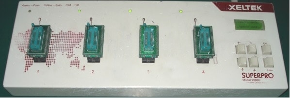
First. “M37544G2A(SP)@SDIP32“ Select the chip model in the programming software. Connect to the Sirte 9000U programmer, open the software “SUPERPRO 9000U“, click “select device“, select “RENESAS” for the manufacturer name, select “M37544: “M37544G2A(SP)@ SDIP32“
- M37546: “M37546G4(SP)@SDIP32“
- M38503: “M38503G4A(SP)@SDIP42””,click “confirm” ;
Second. Start loading the program, click “Load File“, select the target file, click “Open“, then “Confirm“, load the sample into the writer. Click “Verify” to verify, and click “Edit Auto Burn“ displays shown in the box. Select “program“ and click “Add“; select “verify“ and click “Add“. The automatic burning method will add “program“ and “verify“. Click “Options” to pop up a drop-down dialog box, select “Mass Production Mode“; click “Auto” to start automatic programming. After programming is complete, replace the chip, and then cycle programming.
2. Renesas M38D24 program burning :
1)、Before working, connect the writer head to the writer and insert the USB plug on the Sirte 3000U writer into the USB port on the computer host, and the power indicator on the writer will be on.
2)、 Double-click the “SUPERPRO USB series” shortcut icon on the computer monitor to enter the main programming interface. Click “Select Device“, select “RENESAS” for the manufacturer name, select “M38D24G4FP@TQFP64” for the device name, and click “OK“.
3)、 Start loading the program, click “Load File“, select the target file, click “Open“, and then “Confirm“. Load the sample into the writer, click “Verify” to verify. After the verification is correct,click “Edit Auto Burn” to display the dialog box shown in the box.Select “program” and click “Add“. select “verify” and click “Add“. The automatic burning method will add “program” and “verify“. Click “Options” to pop up a drop-down dialog box, select “Mass Production Mode“; click “Auto” to start automatic programming. After programming is complete, replace the chip, click “Auto” again to program, and then cycle programming.

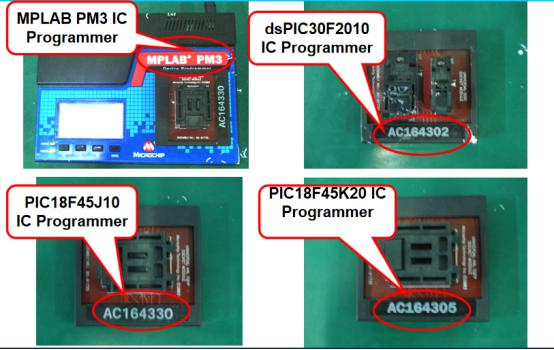
3. PIC18F45J10, dsPIC30F201, PIC18F45K20Program burning:
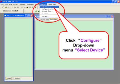
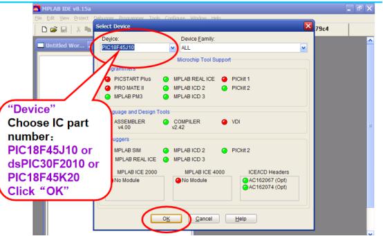
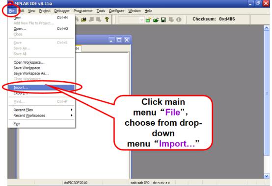
1)、Before proceeding with any work, first select the corresponding programming head according to the type of chip to be burned and place it on the bottom board of the writer (MPLAB PM3). Connect the power of the writer, then turn on the power and open the software “MPLAB IDE v8.5a“. Select the corresponding chip model, click “Configure” drop-down menu, and select “Select Device“. Select the corresponding chip model in the device item: PIC18F45J10 or dsPIC30F2010 or PIC18F45K20 and click “OK“.
2)、Load program: Click “File” on the main menu, select “Import…” from the drop-down menu, select the target file, and click “Open“. Click “Configure” on the main menu and select “Configuration Bits…” in the drop-down menu to configure. When configuring, click “Configuration Bits set in code” to remove the configuration protection, click “OK“, and then start the configuration. After the configuration is complete, click “Configuration Bits set in code” to lock the configuration word.
3)、Click “Programmer” on the main menu, select the drop-down menu.
“Select Programmer” click “7. MPLAB PM3” in the menu.
Then click “Programmer” on the main menu, select the drop-down menu
“Enable Programmer“.
4)、Click the “Program” shortcut in the main menu to start programming. After it’s successful, replace the chip and click the “ENTER” button on the programmer to start offline programming.
Introduce step by step of MPLAB IDE v8.5a IC Programmer software
Click open MPLAB IDE v8.5a IC pr


PIC18F45J10 Configuration standard

dsPIC30F2010 Configuration Standard

PIC18F45K20 Configuration Standard

PIC18F45K20 Configuration Standard


4.TMP 86FH46ANG online program burning:
First. Connect the programmer to the computer with a USB cable, connect the power cord, plug in the power plug, and turn on the device switch on the programmer.
Second. Double-click the “GTPRO” shortcut icon on the computer monitor to enter the main interface for programming. If the connection is wrong, the display is as shown in the middle figure. Check the line connection status, start again until the display is shown on the right.
Third. Click “Open” in the toolbar, click “OK” in the pop-up dialog box. Select the target file, click “Open”, then click “Options” in the toolbar. Click “Settings” in the drop-down menu, select “Program”, “Verify”, click “OK,” to load the sample into the writer, and click “Verify” to verify. After displaying “verification correct”, replace the blank chip to be programmed. Click “AUTO” to start programming. After the programming is successful, it will display “Verification correct, verification code=XXXXXX”, make a mark, replace it with a new chip, and repeat the operation.


GET IN TOUCH
Send Us a Message and Learn More About Our Services
Leave a request and we will contact you as soon as possible